
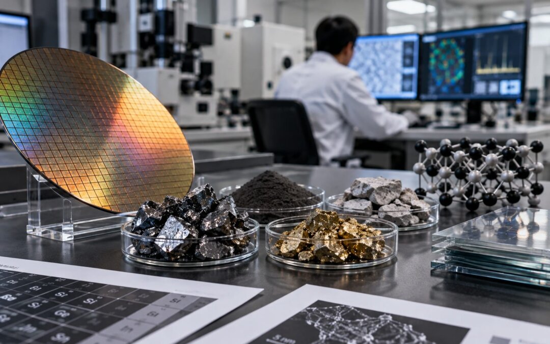
For decades, the technology industry has been built on a remarkably simple idea.
Make transistors smaller.
Smaller transistors allowed engineers to place more computing power onto a chip. More computing power produced faster computers, smaller devices and eventually the smartphones and cloud services we use today.
Silicon made this possible.
But continuing to shrink silicon transistors is becoming increasingly difficult.
That does not mean silicon is about to disappear.
It does mean researchers are searching for new materials and new architectures that could extend computing beyond some of silicon’s physical limitations.
Among the most interesting candidates are two-dimensional materials such as graphene and molybdenum disulfide.
The next computing revolution may depend as much on materials science as computer science.
Silicon Has Been Extraordinary
It is difficult to overstate silicon’s importance.
Silicon is abundant, relatively inexpensive and has electrical properties that make it ideal for manufacturing transistors.
More importantly, semiconductor manufacturers have spent decades learning how to produce silicon devices at enormous scale and extraordinary precision.
Replacing that infrastructure is not easy.
This is why discussions about the “end of silicon” can be misleading.
Silicon is likely to remain the foundation of computing for many years.
The more realistic question is whether other materials can be added to silicon systems to overcome particular limitations.
Recent research suggests that may be possible.
The Problem With Going Smaller
Modern transistors are already extraordinarily small.
As dimensions approach the atomic scale, engineers encounter physical problems that become increasingly difficult to manage.
Electrons can leak through barriers.
Heat becomes harder to control.
Electrical resistance increases.
Manufacturing becomes more complex.
The conventional approach of simply shrinking everything becomes less effective.
Researchers are therefore looking at materials that behave differently at extremely small dimensions.
Two-dimensional materials are especially interesting because they can be only one or a few atoms thick.
Graphene is perhaps the best-known example.
But graphene is only one member of a much larger family.
Transition-metal dichalcogenides such as molybdenum disulfide, usually written as MoS2, have attracted substantial attention because they possess electronic properties that can be useful for transistors.
A Transistor Only a Few Nanometers Long
Recent research illustrates how quickly this field is developing.
In September 2026, researchers reported wafer-scale MoS2 transistors with physical channel lengths below five nanometers.
The devices achieved an on-off ratio greater than one million and demonstrated switching characteristics that researchers argue could extend transistor scaling beyond some conventional silicon limits.
Another research group reported wafer-scale MoS2 transistor arrays in July using an atomically thin graphene gate and a nanometer-scale channel.
The researchers were also able to integrate the devices into basic logic circuits, including NAND and NOR gates.
That last part is important.
Demonstrating an unusual transistor in a laboratory is interesting.
Showing that it can be manufactured across a wafer and incorporated into actual logic circuits moves the research a step closer to practical electronics.
There is still a very long distance between a laboratory demonstration and a semiconductor fabrication plant producing billions of reliable devices.
But the direction is significant.
Graphene May Play a Different Role
Graphene has been discussed as a potential semiconductor material for years.
Its electrical and thermal properties are remarkable.
Electrons can move through it extremely quickly, and it conducts heat exceptionally well.
But pristine graphene lacks the natural bandgap required for the type of digital switching used in conventional logic transistors.
That limits its usefulness as a direct replacement for silicon in many applications.
Researchers are therefore exploring other roles.
Graphene can potentially serve as an interconnect, electrode, sensor or heat-management material.
It can also be engineered into narrow structures known as graphene nanoribbons, where its electronic behavior changes.
A 2026 review in Nature Nanotechnology highlighted the potential role of graphene and other two-dimensional materials in the back end of advanced chips, including interconnects and power-delivery systems. These materials could potentially reduce electrical resistance and improve heat dissipation as conventional metal connections become more difficult to scale.
That illustrates an important point.
The future may not involve choosing between silicon and graphene.
It may involve combining them.
Chips Could Become Three-Dimensional
New materials are only part of the solution.
Chip architecture itself is changing.
Traditional integrated circuits have largely been built across a flat surface.
Increasingly, manufacturers are stacking components vertically.
This allows logic and memory to sit closer together, reducing the distance data must travel.
That can improve both speed and energy efficiency.
Researchers reported a significant demonstration of monolithic three-dimensional integration using silicon transistors in May 2026.
Two-dimensional materials could eventually make this approach even more interesting.
Because they are extremely thin and can potentially be processed at relatively low temperatures, researchers are studying whether they can be added in layers above conventional silicon electronics.
The result could be computing systems that grow upward rather than simply shrinking sideways.
Energy May Matter More Than Speed
For decades, consumers measured computing progress primarily through speed.
Today, efficiency is becoming just as important.
Artificial intelligence has dramatically increased the amount of computation performed in data centers.
That computation consumes electricity and generates heat.
Future materials therefore need to do more than make transistors smaller.
They need to reduce the energy required to move and process information.
Recent materials research increasingly focuses on this problem.
Scientists are exploring two-dimensional semiconductors, ferroelectric materials and engineered interfaces that could allow memory and computation to operate more closely together while consuming less energy.
This may eventually change how we define a better computer chip.
The winner may not simply be the processor capable of performing the most calculations.
It may be the processor capable of doing useful work using the least energy.
There May Be No Single Successor
People often ask what material will replace silicon.
The answer may be that nothing completely replaces it.
Future chips could contain silicon transistors, two-dimensional semiconductors, graphene interconnects, specialized memory materials and entirely new device structures.
Different materials may perform different jobs.
That would not be unusual.
Modern technology is already built from complex combinations of materials selected for very specific properties.
Semiconductor manufacturing may simply become more diverse.
Silicon established the foundation for the modern computing industry.
Its next chapter may involve learning how to combine that foundation with materials that behave better when electronics become extremely small, extremely dense and extremely energy intensive.
The search for what comes after silicon may therefore have an unexpected answer.
It may not be one new material.
It may be an entirely new way of building computers.